Domestic 14nm "mini lithography machine" successfully developed! HuiRan Microelectronics overcomes the bottleneck in wafer online metrology: 10x efficiency improvement
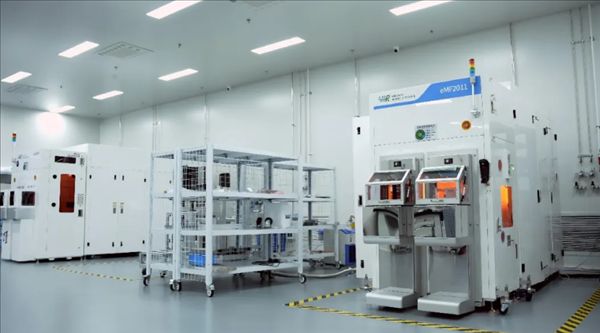
Semiconductor metrology and inspection equipment company Huiran Microelectronics recently disclosed the latest progress in the domestic development of its Critical Dimension Scanning Electron Microscope (CD-SEM). CD-SEM, known in the industry as the "mini lithography machine," is the semiconductor equipment category with the second-lowest domestic localization rate, second only to lithography machines.
Dr. Wang Zhigang, Chairman of Huiran Microelectronics, noted in a media interview that CD-SEM localization faces three core barriers: interdisciplinary technology integration, experience and know-how accumulation, and supply chain supporting capabilities.
Based on its common electron beam technology platform, Huiran Micro has established a dual-line product layout covering "semiconductor + pan-semiconductor/scientific instruments," with product lines spanning CD-SEM, Electron Beam Inspection (EBI) equipment, Scanning Electron Microscopes (SEM) for research, and Focused Ion Beam (FIB-SEM) systems, compatible with both 12-inch and 6/8-inch wafer applications across multiple scenarios.
Huiran Microelectronics has successfully developed 14nm R&D-grade and 22nm production-grade CD-SEM metrology equipment for 12-inch wafers, overcoming the bottleneck in online metrology for advanced process wafers. Multiple metrology and inspection tools have reportedly been deployed and are running stably on production lines of domestic customers using mature process nodes.
Notably, Huiran Microelectronics is the first to introduce AI technology into its microscopic metrology analysis system. Through deep learning, it enhances single-frame scanned images to a quality level approaching that of 64-frame imaging, potentially boosting production efficiency in relevant process segments by more than tenfold.
The company will unveil several major new products at the 14th Semiconductor Equipment, Materials and Core Components Exhibition, including 14nm R&D-grade and 22nm production-grade 12-inch wafer CD-SEM systems, photomask critical dimension metrology equipment, and an AI-electron beam metrology technology platform. Some of these products are domestic firsts.
In terms of industry collaboration, China Resources Microelectronics and Huiran Microelectronics have signed a strategic cooperation agreement to focus on the domestic substitution of semiconductor metrology and inspection equipment, jointly tackling key technical challenges and advancing the industrialization of innovative outcomes.
Wang Zhigang stated that the next 3 to 5 years will be an accelerated catch-up period for the domestic electron beam metrology field. Huiran Microelectronics will leverage a four-tier collaborative strategy involving "end users, research institutions, industry partners, and upstream supply chain" to drive the self-reliant and controllable development of domestic semiconductor metrology equipment.
Related Articles
Huawei Mate 90 series has entered the network: directly marked as 5G! Debuting the Taolaw-compliant Kirin chip.
2 days ago

Xiaomi 18 Fold Three Major Debuts: Xuanjie 03 + ChangXin LPDDR6 Memory + HyperOS 4
2 days ago

Acer launches Aspire G 3D 16 laptop: Strix Halo chip with glasses-free 3D display support.
2 days ago