A milestone for domestic flagship SoCs! Technical analysis of Xiaomi's Xuanjie O3
Xiaomi held a Xuanjie chip technology briefing in Beijing, officially unveiling three self-developed chips: Xuanjie O3, O100, and D100, targeting flagship smartphone SoCs, on-device AI acceleration, and intelligent driving scenarios respectively. The "triple-chip launch" together maps out a full AI computing landscape spanning "pocket to cockpit, living room to factory" for its human-vehicle-home ecosystem.
**Xuanjie O3: Flagship AI SoC, AnTuTu Score Exceeds 5.2 Million**
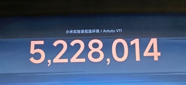
The O3 is Xiaomi's second self-developed high-end flagship SoC, built on a 3nm process with transistor count increasing from 19 billion on the O1 to 24 billion. Xiaomi's lab-reported AnTuTu comprehensive score is 5,228,014, making it the first mobile flagship platform in the industry to break the 5-million mark.
Additionally, the new chip has been almost entirely redesigned at the architecture level. The CPU adopts a ten-core "all-big-core" configuration with 6 super-large cores plus 4 large cores, reaching a peak clock speed of 4.35GHz.
GeekBench 6 scores 3,945 single-core and 15,221 multi-core, representing increases of 31% and 60% over the previous generation—highly significant gains. Meanwhile, power consumption in daily-use scenarios is further reduced by 25%, balancing performance and efficiency.
For graphics, the O3 debuts the next-generation G2-Ultra NX GPU, maintaining a 16-core ultra-large configuration. Traditional graphics performance is up 85% over the O1, ray tracing performance improves by 182%, and power consumption at equivalent performance drops by up to 64%. The Aztec frame rate reaches 213fps, a 94% improvement over the previous generation—a generational leap.
In imaging, the Xuanjie O3 also delivers massive upgrades. The fifth-generation ISP supports a single camera with up to 432MP, with internal image signal processing at 24-bit width. AI RAW-domain noise reduction brings night video up to 4K/60FPS. The DPU extends screen zone tone mapping to more scenarios, improving low-light readability and enhancing HDR source display. The VPU adopts a separate encode/decode architecture, boosting video editing export speed by 20% and debuting H.266 hardware decoding in the Android space.
The security module has also been fully restructured, earning national cryptography and CCRC EAL5+ security certifications. Baseband communication performance is on par with mainstream flagship integrated solutions, with 5G comprehensive power consumption reduced by over 20% compared to the previous generation.
Memory and cache also see significant upgrades this time. The O3 integrates a total of 60MB of on-chip cache, with 16MB of SLC addressing the previous generation's shortfall. It also debuts LPDDR6 support, delivering 113.8GB/s memory bandwidth—48% higher than the previous generation.
With upgraded cache and memory bandwidth, the Xuanjie O3 also adjusts internal data transfer. It adopts a unified fused bus architecture that reduces protocol conversion between modules, paired with top-metal-layer data paths and data prefetching. Data shows the unified transfer protocol cuts protocol conversion overhead by 75%, with memory access latency as low as 82ns, reaching industry-leading levels.
On scheduling, Xiaomi emphasizes that roughly 30% of daily stutters stem not from insufficient compute but from tasks queuing for resources. The Xuanjie O3 adds a hardware scheduling control unit with a full-stack QoS mechanism, allowing critical tasks to pass through every stage with priority. Combined with real-time monitoring of load, temperature, and voltage plus scenario prediction, global resource feedback completes in as fast as 1ms, delivering energy-efficiency gains of generally over 20% in high-frequency usage scenarios.
On AI—a key focus—the Xuanjie O3 integrates AI compute units into major modules like CPU and GPU to handle lightweight AI tasks such as translation, audio-video understanding, and graphics processing, reducing cross-module data transfer and extra power consumption.
Large models remain handled by the NPU. The Xuanjie O3 features a 4-core NPU with 200 TOPS tensor compute and adds a SIMT-architecture Vector unit providing 3.13 TFLOPS of vector compute.
For on-device large models, the Xuanjie O3 is jointly optimized with Xiaomi MiMo, using 5-value quantization and hardware Huffman lossless compression to reduce model data size. According to data shared at the event, model inference speed is 45% faster than mainstream flagship SoCs.
**Xuanjie O100: 1.22TB/s High Bandwidth, Solidifying the Hardware Foundation for the Agent Era**
Beyond the Xuanjie O3, the briefing also introduced two additional chips: the Xuanjie O100 and Xuanjie D100. The O100 is a 6nm on-device AI acceleration chip that can run on-device large models alongside the Xuanjie O3, completing local AI computation in weak-network or offline environments.
The O100 uses 3D Wafer-on-Wafer stacking, connecting two DRAM wafers and one NPU compute wafer via Hybrid Bonding technology. The chip contains 2.58 million bonding nodes with a bonding pitch of 1.4µm. Between the top-layer DRAM and compute wafer, 28,672 connection paths are arranged, offering higher interconnect density and shorter data paths than traditional external memory solutions.
According to Xiaomi's data, the Xuanjie O100 achieves 1.22TB/s memory bandwidth—roughly 16 times that of mainstream phone memory—with on-device large model inference speeds up to 330 tokens per second. The chip also integrates a 14-core dedicated NPU for large models and employs an XRING HB-Matrix high-bandwidth matrix bus.
In manufacturing, the O100 does not use the traditional MicroBump approach. The TSV diameter for Hybrid Bonding is 0.7µm, and the three-layer chip stack uses F2F metal-layer direct connection. High-temperature bonding can easily cause wafer warping and cracking. Xiaomi says the team spent about six months iterating the chip layout and filed multiple patents around the F2F metal-layer direct connection architecture.
**Xuanjie D100: China's First 3nm Intelligent Driving Chip, Running 200B Large Models On-Device**
The Xuanjie D100 uses a 3nm process and is positioned as a high-compute AI chip for intelligent driving. It features a 20-core high-performance CPU and a 16-core NPU, making it China's first 3nm intelligent driving chip.
Beyond running autonomous driving algorithms, the D100 supports larger-scale local AI computation. A single chip supports up to 160GB of memory and can deploy large models exceeding 200B parameters. Multiple D100 chips can also perform joint computation via the Xuanjie high-speed interconnect bus.
**Final Thoughts:**
According to current plans, the Xuanjie O3 will debut in September with the Xiaomi 18 Fold. Both the Xuanjie O100 and D100 have completed development and are expected to enter commercial use next year.
A year ago, the Xuanjie O1 proved Xiaomi's capability in self-developed flagship SoCs. Now, with the O3, O100, and D100 unveiled simultaneously, Xuanjie's application scope has expanded from smartphones to on-device AI and intelligent driving, beginning to cover the computing needs of Xiaomi's full "human-vehicle-home" ecosystem.
Self-developed SoCs have never been an easy path—especially at flagship level, where R&D, mass production, tuning, and subsequent iteration all require long-term investment. Based on the technical details disclosed this time, Xuanjie has entered the validation stage of real product capability.
Next month, the Xuanjie O3 will debut with the Xiaomi 18 Fold. Its real-world performance, efficiency, and AI experience will serve as an important benchmark for evaluating this generation of Xuanjie.
Related Articles

Huawei phone users have finally got what they've been waiting for! The HarmonyOS trial beta version of NetEase Cloud Music is now available.
about 3 hours ago

The price after discounts is 6544 yuan! Lenovo ThinkPad E14 2026 laptop is now available: Core 5 320 + 512GB
about 4 hours ago