Ensuring Kirin production capacity based on Huawei's Tao's Law! The largest domestic advanced packaging financing has landed: monthly output of 100,000 wafers.
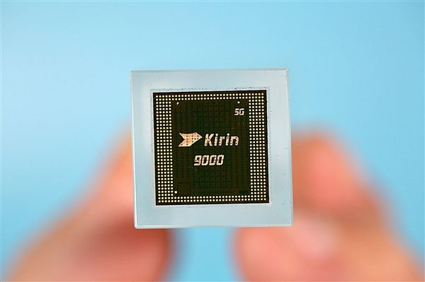
Entering next month, the Kirin 2026 chip, built on Huawei's Tao's Law technology system, will officially meet consumers. Once this long-polished domestic flagship chip is released, it is bound to once again reshape external perceptions of the ceiling of domestic semiconductor technology.
For Huawei, the stable supply capacity of the Kirin 2026 chip this time is not closely tied to the strength of traditional high-end chip manufacturing process nodes. The core support comes entirely from the advanced chip packaging capabilities that domestic players have rapidly caught up on in recent years, using breakthroughs on the packaging side to directly bypass external restrictions on high-end process nodes.
To further expand the domestic production capacity base for advanced chip packaging, Hubei Xingchen Technology Co., Ltd. recently completed a Series A financing round totaling nearly 5 billion yuan. This round directly set a new record for single-round financing in the domestic advanced packaging sector, and the company simultaneously unveiled a long-term development blueprint targeting a monthly production capacity of 100,000 wafers and annual revenue of 10 billion yuan.
Currently, the second-phase pilot line at Xingchen Technology is busily moving in various core process equipment, with full line connectivity expected by September this year. Combined, the first and second phases represent a total investment exceeding 7 billion yuan, with planned monthly capacity at the current stage reaching 20,000 wafers. This has already established the largest and most technologically advanced high-density integrated packaging pilot and small-batch mass production platform in the country.
The Jiulonghu industrialization base, also located in Wuhan's Optics Valley, is accelerating construction progress, with official production launch expected by the second half of next year.
In May this year, Huawei officially unveiled the Tao (τ) Law, marking the first time a Chinese company has proposed a brand-new underlying principle for industry development in the global chip sector. The core manufacturing foundation of this technical roadmap is domestically controlled, independently developed advanced packaging technology.
Leveraging Xingchen Technology's advanced packaging capabilities, engineers can integrate storage chips and logic chips of different process nodes together in a high-density, building-block-like manner, forming a more compact interconnect structure than traditional single-chip solutions. The resulting AI inference bandwidth is directly improved by one to two orders of magnitude compared to traditional single-chip architectures, with overall performance sufficient to match or even surpass flagship chips built on overseas 7nm and 5nm processes.
From the introduction of Tao's Law to the rapid establishment of a full-chain advanced packaging capacity echelon, this entirely new roadmap—completely breaking free from reliance on overseas semiconductor technology paths—is steadily taking firm control of the development initiative of China's semiconductor industry. The upcoming official debut of the Kirin 2026 is merely the first clear signal in the process of domestic chips overtaking through a detour.
Related Articles
Huawei phone users have finally got what they've been waiting for! The HarmonyOS trial beta version of NetEase Cloud Music is now available.
about 3 hours ago
The price after discounts is 6544 yuan! Lenovo ThinkPad E14 2026 laptop is now available: Core 5 320 + 512GB
about 4 hours ago